In this focus we will report on the first single electron transistors (SET) fabricated on silicon/germanium heterostructures whose critical dimensions are in the nanometer scale. The evolution of fabrication techniques in large scale integrated circuit (LSI) have lead to reduction of the size of the electronic devices into the submicron scale. In parallel a large increase in the circuit operating speed and device density is observed. CMOS technology is presently used in microelectronics and requires thousands of electrons to define each bit. The continuos miniaturization of the electronic devices makes the statistical fluctuations in the electron number increasingly significant preventing a clear definition of the bit state. In SETs, due to the coulomb blockade effect, the electron transport can be controlled with the single electron precision. The SETs can be then used in circuits where the bit is defined by only a few electrons.
In the Photonic and Nanotechnolgies Institute SET devices, based on high mobility two-dimension electron gas, obtained in SiGe modulation-doping heterostructures, are fabricated by using a top down approach based on electron beam lithography. The peculiarity of the work relays in the use of SiGe heterostructures grown on silicon by epitaxy. The SiGe has the advantage of being compatible with the silicon technology used for commercial electronics and at the same time the heterostructure allows to fully exploit the advantageous properties of these materials.
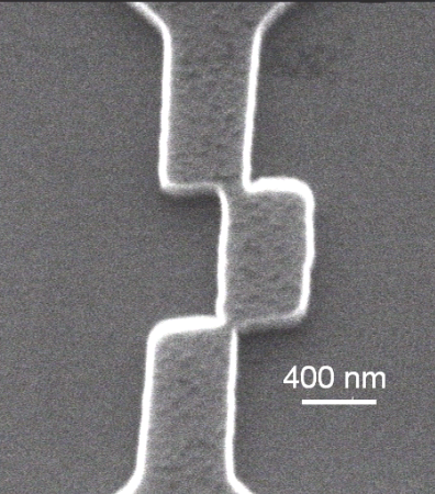
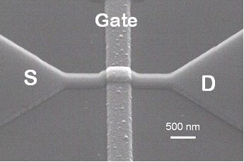
The architecture proposed and used for the device fabrication, based on a "bend-wire" geometry (see figures) is new and potentially scalable with geometric size, giving rise to a possible increase of the working temperature of the transistor.
The tunnel barriers that define the active region of the device (the island) are formed by constrictions in the wire, obtained by a shift of the central area of the wire itself. The amount of the shift is smaller than the wire width. The island is connected, through the two constrictions generated by the shift, to the ends of the wire that act as source and drain terminals. The electrical characterization of these SET has been performed at T= 4.2K and the stability plot with diamonds shapes typical of a single electron transistor has been observed. Charge effects have been observed up to 40K, a temperature far larger than the liquid helium boiling point.
The investigation of the transport properties demonstrate both the peculiar effects of single charge and the stochastic nature of coulomb blockade in this material.
Immagini:


