Over recent years there has been a tremendous drive towards computer miniaturization.
At present the smallest components of a commercial microelectronic device are about 130 billionths of a metre (nanometre). Smaller dimensions would provide more powerful computers and reduce energy consumption, a fundamental issue in the explosive market of wireless communication, including mobile phones, portable video and audio players, laptops, etc.
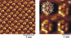
Further, significant miniaturization will require manipulation of materials at the molecular or even atomic level, i.e., less than a nanometre. The science which studies phenomena on this scale is called nanoscience. At ISOF, techniques such as Scanning Tunneling Microscopy (STM) and Scanning Force Microscopy (SFM) are used to visualize the structure of atoms and molecules (Figure 1)[1]. In these techniques a tiny probe scans over the surface measuring local physical properties such as electron transfer or the force of surface-tip interaction.
These microscopies can operate in different environments (vacuum, ambient, gas stream or liquid) allowing one to initiate chemical reactions on a surface and follow them, with molecular resolution. For example, using STM we have monitored the chemical transformation of single hydrocarbon molecules on a surface [2] and have visualized, using SFM, individual optically-active rod-like macromolecules, useful for LCDs, gaining insight into their structural properties [3].
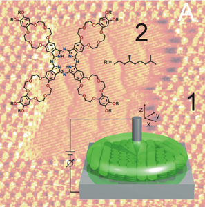
The tip of the SPM can also be utilized to manipulate nanostructures at the molecular scale such as the methodology for "writing" on a layer of organic molecules by changing their orientation at the surface (Fig. 2A). This offers a significant increase in data storage density (HD, CD-ROM, DVD) [4].
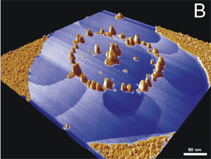
In the field of electronics we can follow the behaviour of silicon atoms on very clean surfaces, prepared in ultra-high vacuum (UHV) at pressures of 10-13 atm (almost as low as that in outer space). Small molecules can be used to stimulate and control the growth of nanostructures on silicon surfaces [5]. Under the influence of these molecules silicon atoms move and rearrange spontaneously forming different nanoshapes such as islands and lines. This approach, producing small circular arrangements of Si-on-Si nanostructures (Fig. 2B), will also allow the development of a new generation of organic-silicon hybrid devices [6], where the organic molecules can self-organize and react with silicon surfaces to produce single-molecule devices, nanoscopic sensors for biological applications, labs on a chip, etc. The possibility of exploiting SPM to control the properties of single molecules and of their supramolecular aggregates is of paramount importance for these future technological developments.
Vedi anche:
Immagini:


