Photovoltaic devices, which directly convert abundant light into solar electricity, are important for the implementation of renewable energy supply systems. Today, silicon-based modules are dominating the photovoltaic market, but various emerging technologies based on thin-film inorganic semiconductors, dye-sensitized materials and organic materials are rapidly progressing.
Thin-film photovoltaic devices can be manufactured on flexible substrates, enabling the employment of industrial roll-to-roll deposition techniques.
Besides cost-reduction, flexible photovoltaic devices allow new opportunities in areas such as building integration or portable electronics. However, the conversion efficiency of flexible solar cells has always been until now significantly lower compared with photovoltaic devices on rigid substrates.
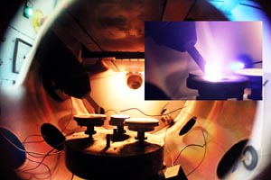
Amongst thin-film technologies, CIGS has yielded maximum conversion efficiencies of up to 20.8% using rigid soda lime glass (SLG) as a substrate. SLG substrates were so far favoured because they allow high processing temperatures of 600°C or even more, have a coefficient of thermal expansion similar to CIGS, and provide the right amount of Na necessary for high-efficiency devices directly during film growth. In contrast, polyimide film as a flexible substrate can withstand processing temperatures only of well below 500 °C, posing significant constraints on growing high quality CIGS layers, have a large thermal mismatch with CIGS and do not contain alkaline elements, which necessitates an adequate extrinsic supply method. Moreover multi-stage thermal co-evaporation, by which the current 20.8% lab-record efficiency was achieved, is generally considered to be unsuitable for mass production because of its complexity and poor composition reproducibility in large manufacturing systems. Sputtering of metal precursors followed by a post-growth selenization step appears to be a more feasible route for industrial scale up but the unavoidable selenization stage is a major issue in terms of environmental impact (highly toxic H2Se is usually used) as well as the operation costs linked to high temperature processing. In order to overcome the limitations associated with multi-stage deposition, several single-stage processes based on sputtering and co-evaporation have been proposed as more cost-effective alternatives. Reported efficiencies for lab-scale cells are typically lower than 12.5% with the most striking exception of 18% achieved by an in-line co-evaporation process at a substrate temperature = 550 °C. We recently reported the achievement of efficiencies exceeding 15% in lab-scale CIGS solar cells by using a low-temperature (<300 °C) single-stage production process based on pulsed electron deposition (PED). PED is a thin film deposition technique based on high-power electron-beam ablation of a bulk material (target) having the desired composition and stoichiometry. Electron beam pulses of about 100 ns dissipate a power density of the order of 108 W/cm 2 within a depth of the order of 1 μm from the target surface. This causes a rapid non-equilibrium evaporation of all the elemental components of the target and the formation of a plume of ions having a large average kinetic energy. As a result, the deposition of good quality films occurs at a much lower substrate temperature compared to sputtering or single-stage co-evaporation. The two key process parameters whose optimisation allowed us achieve a photovoltaic efficiency > 15% are Na doping and the quality of the targets used for PED deposition. The control of the p-type doping of CIGS films is a crucial process step to optimize the solar cells performance and it is now widely accepted that the level of doping is mainly controlled by the Na concentration and diffusion profile. In our low-temperature deposition process, the desired doping profile is provided by a sodium fluoride (NaF) layer deposited by PED between the Mo back contact and the CIGS absorber. On the other hand, optimized CIGS targets were obtained by a boron-oxide-encapsulated synthesis process starting from elemental species (Cu, In, Ga, and Se with 5 N purity). This process, previously developed for the synthesis of high-purity polycrystalline targets of CdTe and other III-V/II-VI semiconductors, is capable of preserving the starting stoichiometry in the target because molten boron-oxide encapsulation and high inert gas counter pressure (30 ÷ 40 bar Ar) inhibit Se evaporation. Thanks to this improved fabrication route based on PED, cost-effective CIGS solar cells can be deposited at low temperature onto different substrates, even low-melting-point plastics, making the fabrication of flexible solar cell a viable option.
Immagini:

